3D Printed PCBA Test Fixtures

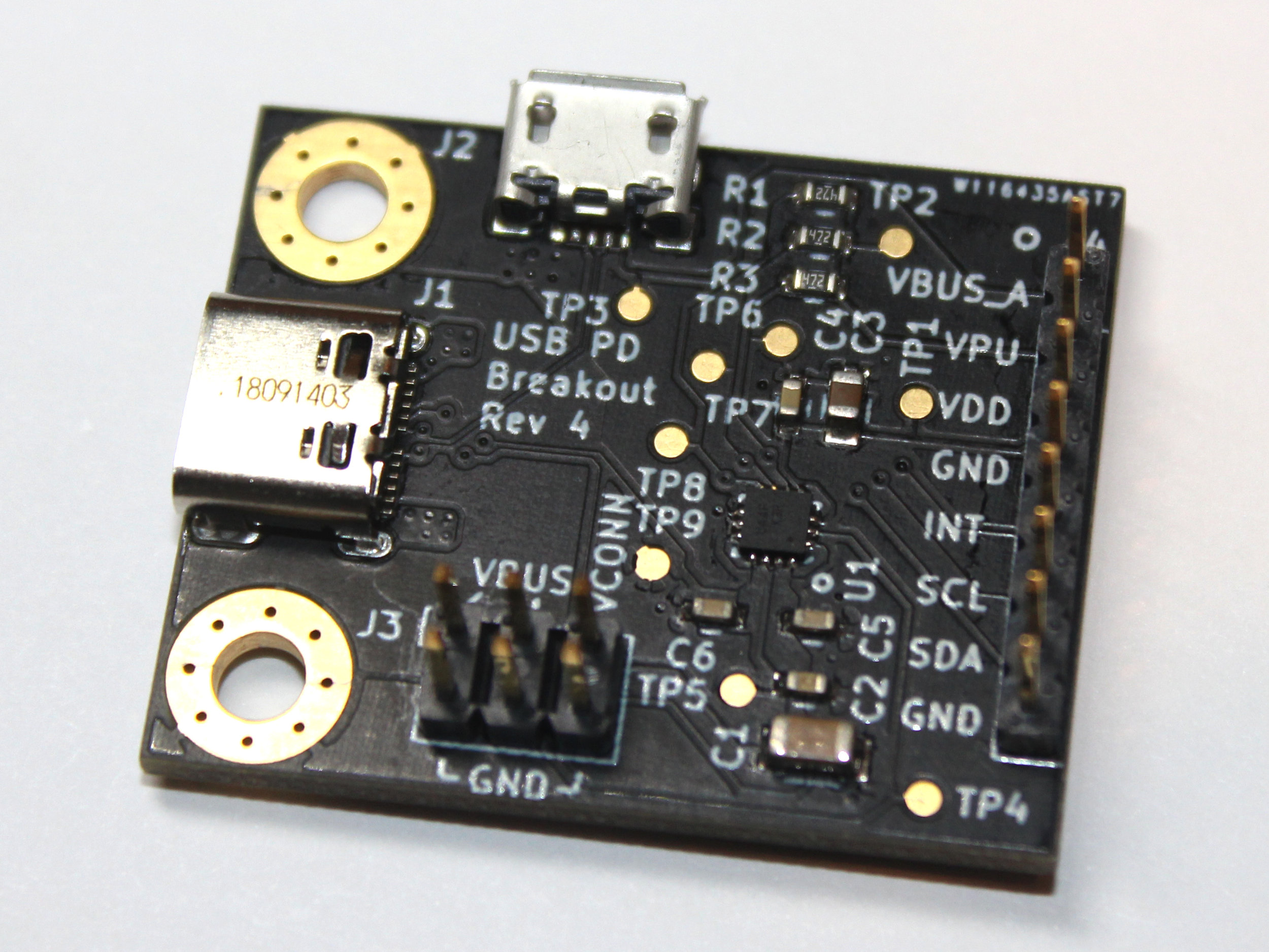
I recently released Rev 4 of my USB-C PD Breakout Board. One of the changes from Rev 3 is better DFM, namely adding testpoints for future fixtures. Testing the Rev 3 boards 100 at a time by manually plugging in jumpers was getting old. Once I had the PCB design locked down and sent for fab, I turned my attention towards prototyping the test fixture. Here are some thoughts and documentation of my process of designing and testing the fixture.

USB-C PD Breakout Board Rev 4

USB-C PD Breakout Board Rev 4

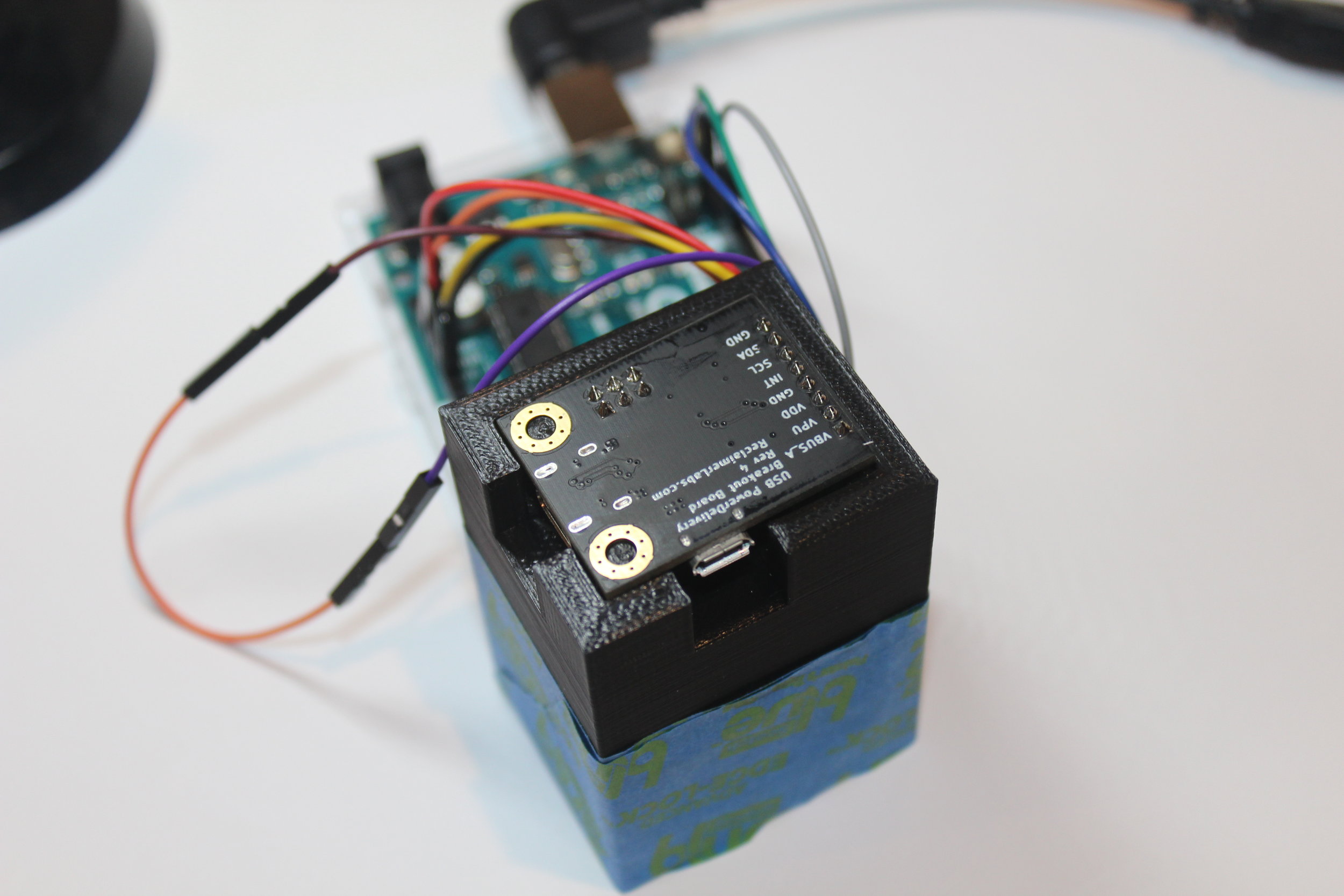
Final version of the test fixture

Final version of the test fixture

Test fixture with PCBA ready

Test fixture with PCBA ready

Initially I considered some other options. I could buy a basic fixture from Aliexpress or similar sites. Those tended to be hundreds of dollars (USD). Then I would still have to fabricate custom plates for top and bottom, probably best done with a laser cutter or CNC router and a kit of pogo pins and spacers. Another option I found was OpenFixture by Tinylabs. It uses OpenSCAD to programmatically generate a box that can be laser cut. Neither of these options were good for me, as I do not have a laser cutter in my lab (yet). However, I do have a 3D printer (on loan from a friend).

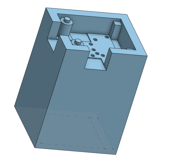
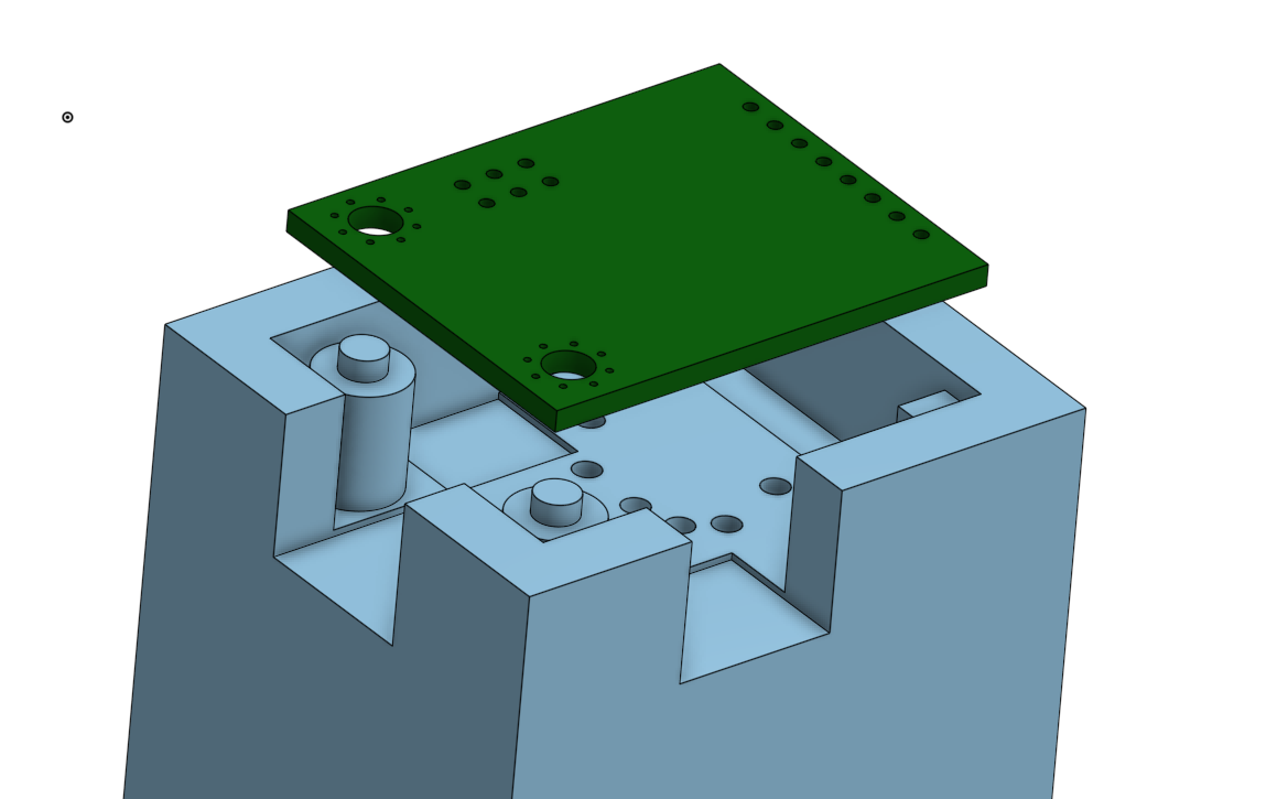
My plan to 3D print the fixture worked out well, though it took a few tries. I used OnShape to capture the mechanical design. Here is a direct link to my design. All my testpoints were on the same side of the PCB, which is pretty much the only way this approach will work. The basic idea was to first create a box, then cut out clearances for the components and such, then add drill holes for the pogo pins. There are four levels of cut-outs. The first was for the really tall headers, second for the USB connectors and their cables, and third for the rest of the SMT components. The fourth level was for the actual board. I added a ring around each mounting hole and two tabs on the back side, which has no mounting holes. This level also leaves behind pins that go inside the mounting holes and the pocket for the outline of the PCB. I also had to consider the height of the pogo pins to make sure they didn’t stick up too high. There are two problems with them being too proud. First is that it take a lot more force to compress the board all the way down to the fixture. Another more serious concern is that you could short something out on your way down. I set my pogo pins to stand about 1 mm below the upper level of the fixture so the board is aligned before it makes contact. Then it has another 1 mm or so until it bottoms out, which is plenty of spring travel to make a good connection.

Final CAD form

Final CAD form

Final CAD with PCBA step file imported for fit check

Final CAD with PCBA step file imported for fit check

Here are some technical notes on using 3D printing for PCBA test fixtures. I’m using the LulzBot TAZ 6 with 3mm black PLA from eSUN. It’s an FDM type 3D printer, which has certain limitations, especially with small, precision detail. I found that the holes it made were undersized and the pins were oversized. I wanted a 3.5 mm (+0/-0.1) pin for the mounting hole, but I had to set it to 3.2 mm in the CAD. For the holes for the pogo pins, I had to set the hole size to 2 mm to get something like 1.5 mm. At first I thought I’d have to drill the holes out after printing, but those numbers create a snug fit on their own. If you go this route, I encourage you to consider starting with a test print to get the settings right for your particular setup.

The pogo pins I used are from Dangerous Prototypes. They don’t make too many guarantees on their quality, but they worked just fine for me. I used the R100-4S sockets and the PA100-J1 pins. I didn’t feel the need to glue them in, but it’s certainly an option to make the fixture more robust, at the cost of making it less serviceable. I tinned each solder cup, then soldered pre-tinned jumper wire leads to connect each testpoint. Everything gets routed to an Arduino. For future designs, I’d recommend making sure you have plenty of space to get a soldering iron in there. It was a little tight this time, and I almost burned my fingers. Another option is to get pogo pins with a connector of some on the back, maybe something that can take a standard female 0.1 inch pre-formed jumper.

3D printing a PCBA test fixture is definitely a viable option, though there are some limitations with the way I did it. It only works if all testpoints are on one side of the PCB, unless you design a top and a hinge. I also have a minimum spacing of 2 mm center-to-center for testpoint placement, although your printer and pogo pins might allow tighter packing. Finally, the PLA material has some limitations. It’s lightweight, which allows the fixture to fly across the table if you’re not careful. Additionally, it doesn’t do well in warm, wet environments, and might degrade long term. If the benefits of being able to print your fixture in a couple hours outweigh these limitation, it’s a great option. Let me know what you think in the comments.

The USB-C Explorer

I've been quiet for a while, mostly because I've been working on a new USB-C board. Actually, the board didn't take the most time; that would be the firmware development. (Never underestimate firmware). The result is a cool piece of gear, a powerful development platform, and a stronger firmware library.

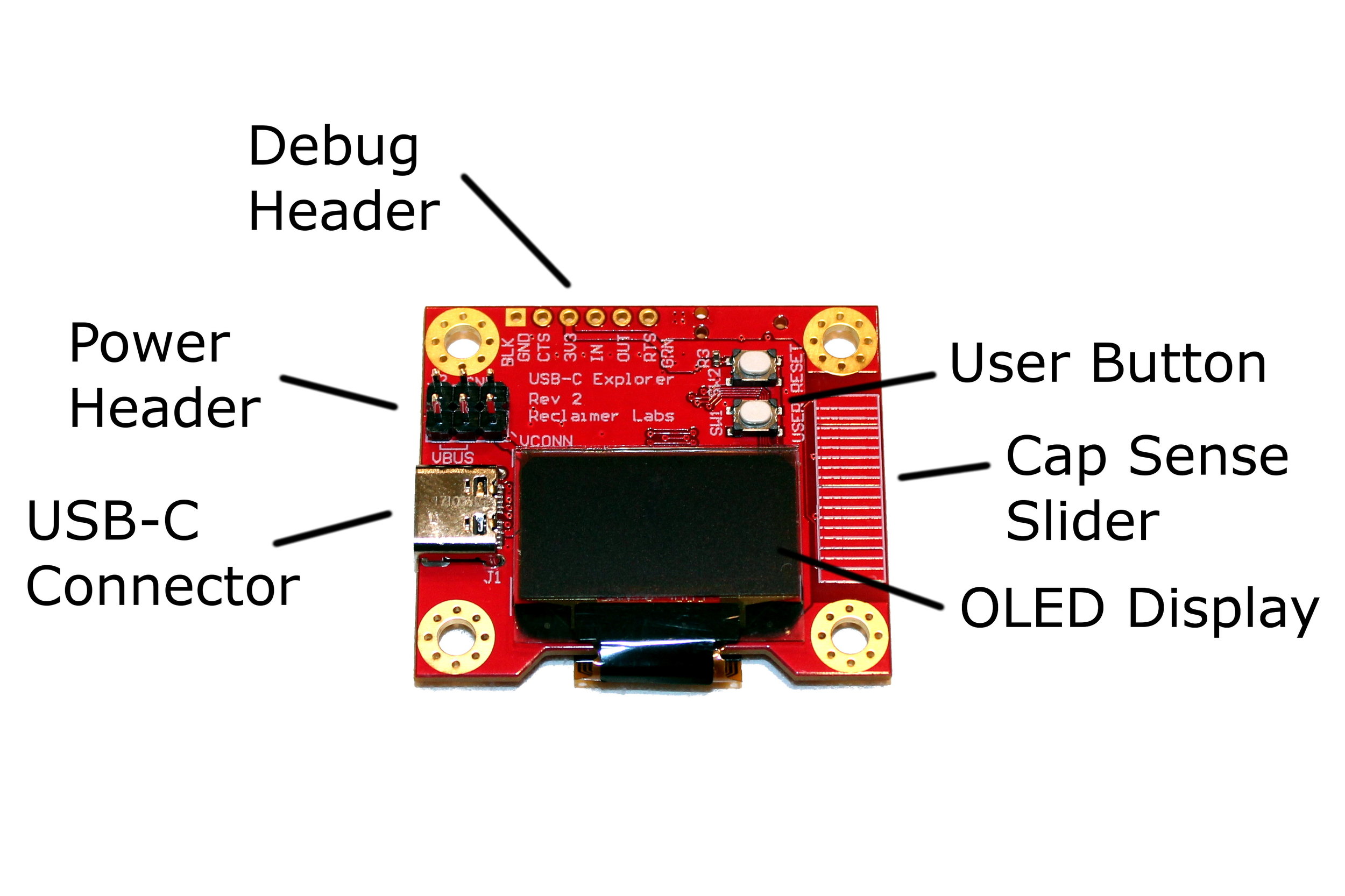
The USB-C Explorer is a development board with everything needed to start working with USB Type-C. It contains a USB-C port controller and Power Delivery PHY chip, a microcontroller, and several options for user interaction. Here are the hardware features.

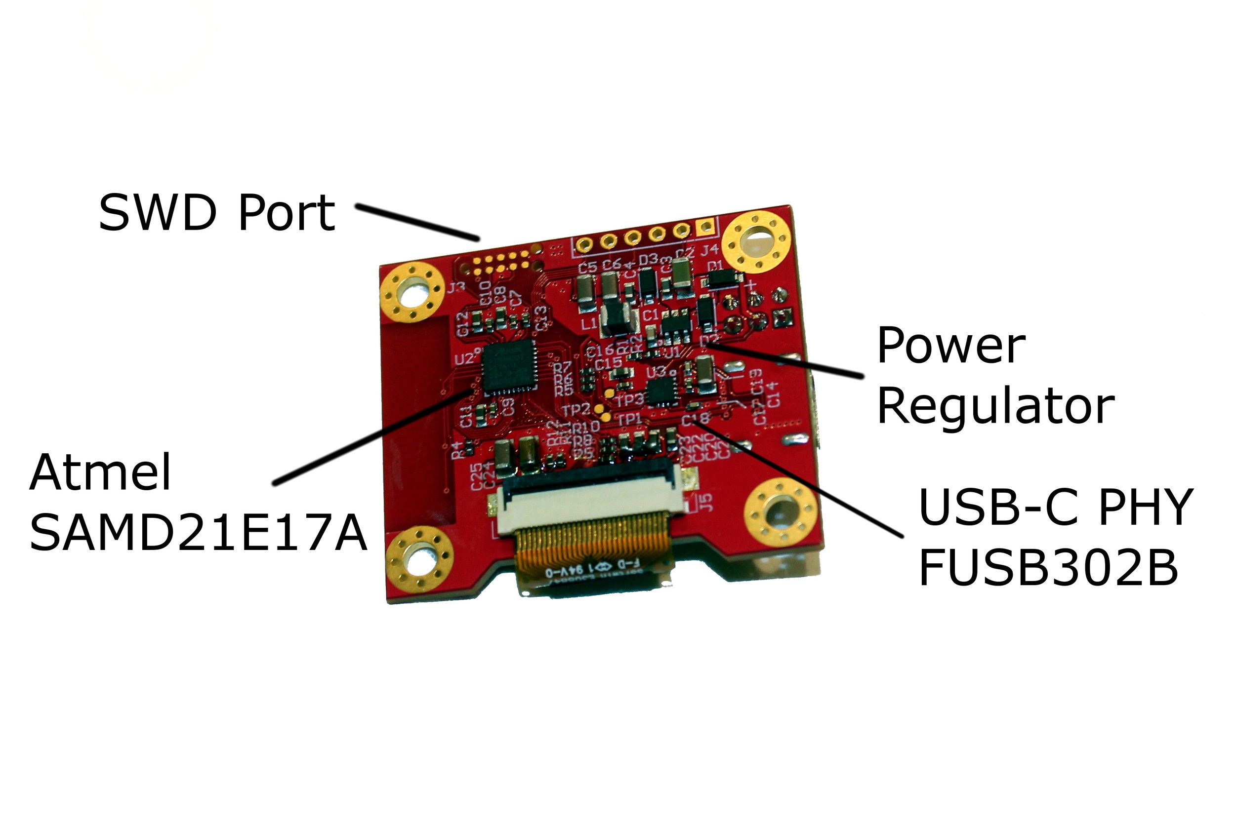
  • SAMD21E17A microcontroller
  • FUSB302B USB PD PHY
  • OLED Display
  • Capacitive-sense slider
  • Power header (up to 5 Amps)
  • Debug port (UART and/or GPIO)
  • SWD connector (Tag-Connect)
  • Reset and User Buttons
  • Onboard regulator, input up to 20 V.

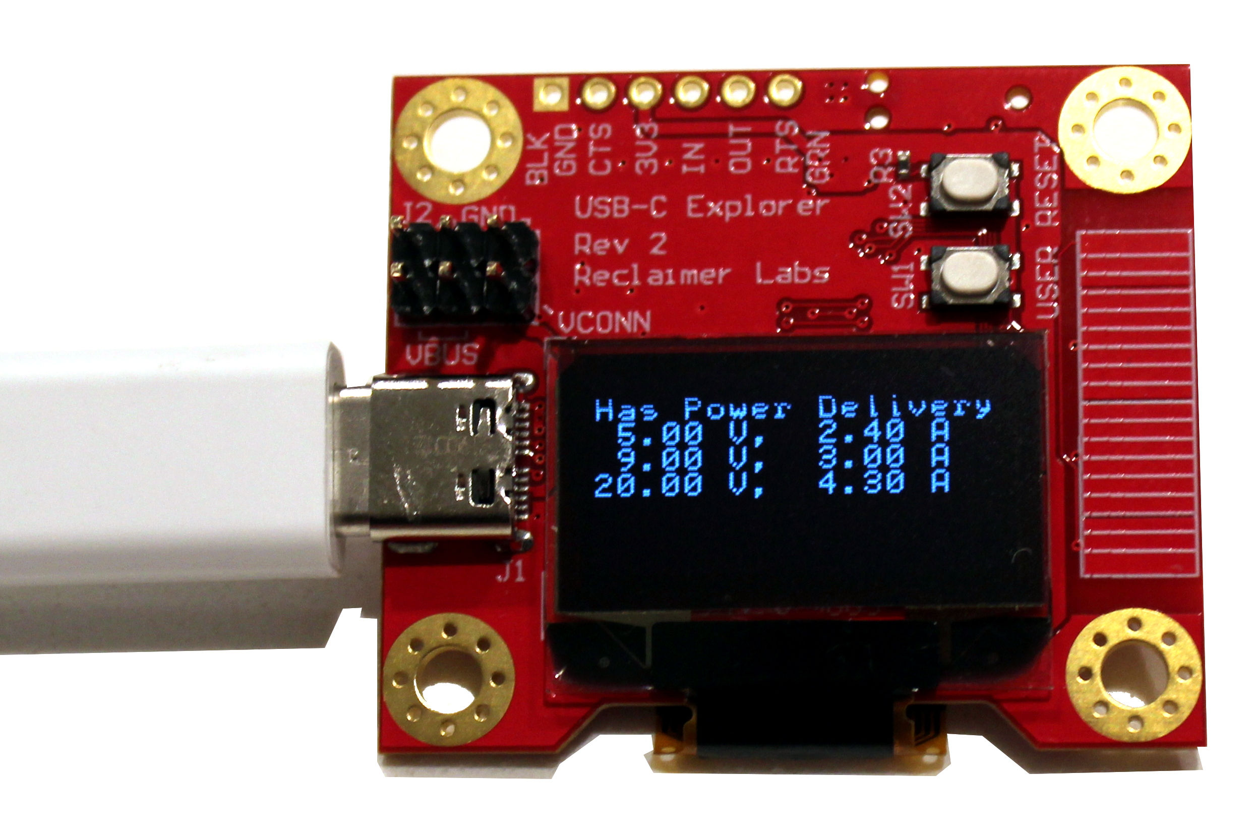
The default firmware will identify as a USB Power Delivery Sink and list out all power capabilities from a corresponding Source. It will then request the highest power option. This voltage will be available on the power header. The example photo shows the capabilities of an Apple MacBook 87W Charger.

The default firmware also includes a USB bootloader. If you hold the User Button during reset, it will show up as a USB Mass Storage Device with a single file "FLASH.BIN". Copy the file to inspect the application firmware. Delete it and replace it with a new .bin file to rewrite the firmware. No programming cable is required.

To use the Single Wire Debug (SWD) function for live debugging, you will need a Tag-Connect TC2050-IDC-NL "plug of nails" cable and clip. You can then use an adapter to something like a Segger or J-Link.

The firmware library has also been redesigned from the ground up to support new platforms. The first of these is support for the Arduino M0. You can find that example here. The intention is that only four files, tcpm_driver.c/h and usb_pd_driver.c/h, need to be modified to support new microcontrollers. New pairs of files such as FUSB302.c/h can be added to support new Type-C Port Managers (TCPM chips).

You can purchase a board from my Tindie store. This design is open source under an MIT license. All hardware designs, documentation, and firmware are freely available. You can find all design files at this github repository. I welcome feedback, so please let me know what you think. In particular, help with firmware would be appreciated.

An Example of USB Power Delivery

Let's take a look at what it takes to get almost 100W of power for a USB-C Easy Bake Oven. In this post, I'll go through the detail of the transactions on the Configuration Channel (CC) when I plug in my oven.

Click to enlarge.

I borrowed a fancy Teledyne LeCroy Mercury T2C USB HS/PD Protocol Analyzer to capture the traffic. You can follow along for free with their software and my saved session. Here is the .usbraw file as well. Once you have everything installed and open the file, you should see this.

The Left device is the Apple MacBook Pro charger. The Right device is my USB-C breakout board. The first packets are from when I plugged in each of the cables. The charger identifies as a Source with a Rp pull-up on CC1. Then my board identifies as a Sink with a Rd pull-down on CC1. Once the connection is established, the charger modulates its current on CC1 to advertised USB Type-C Current at 1.5 Amp. At this point, my board is allowed to draw 1.5 A at 5 V. To get a different voltage requires some transactions using USB Power Delivery.

Click to enlarge.

The charger starts by sending unsolicited Source_Capabilities messages to inform my device about its capabilities as a power source. My firmware ignores these messages, and sends a Get_Source_Cap (packet 86) to request the same information. When the charger sends it again, my board replies with a Request message (90) for the highest available power, which in this case is 5V, 2.4A. The charger sends an Accept message, then a few milliseconds later sends a PS_Ready message to let my board know it can now draw up to 2.4A. Note that every message is followed up with a GoodCRC message.

After that is all settled, one of the devices starts interrogating the cable plug (packets 96-100). SOP' is the start of packet symbol to address the cable plug. All the packets until now have been one device to another using the SOP symbol. As for which device is talking to the cable, it must be the charger. The two devices have an explicit USB PD contract, so only the Source is allowed to communicate with SOP' and SOP'', as noted in Section 4.9 of the Type-C spec. The cable responds with a Structured Vendor Defined Message (VDM). The data objects describe its vendor name, cert status, product ID, USB SuperSpeed support, max Vbus current, latency, and few other miscellaneous bits of data.

Click to enlarge.

Now that the charger knows that the cable can support 5 Amps, it sends a new Source_Capabilities message. In addition to 5V, 2.4A, it now includes 9V, 3A and 20V, 4.3A. Note that the 5V fixed supply is first, as required by the spec. Then all other options are listed in increasing order of voltage, in this case, 27W then 86W. Upon receiving the new capabilities, my board requests the highest possible power. Just like before, the charger sends an Accept message followed by a PS_Ready message.

Finally, the charger sends a Structured VDM to find out more about the device it's charging. Unfortunately, I haven't implemented that part of my firmware, so there's no reply.

That's the end of the transactions. After this point, the Easy Bake oven has the power it needs to run the heater. The Arduino inside is using its on-board regulator to convert the 20V down to 5V to power its microcontroller. In this system, there is no need for further communication. In a more complex version, the oven could send a request for less power when it knows it doesn't need to run the heater. This would allow the source to reallocate that power to other devices. This charger has only one USB-C receptacle and is only connected to my board and the wall, so there's no need for anything like that.

Click to enlarge.

If you want to learn more, I recommend going through the captured transactions with the USB Power Delivery spec open. If you right-click on the Packet number, you will see an option to inspect the raw data. You can select between looking at the 5-bit data that was transmitted on the wire, or the 4-bit nibbles it represents. In 4b mode, you can go through each bit of each message and compare it against the tables in Section 6 of the USB PD spec.

If you want to play around with USB-C yourself, you can buy one of my board on Tindie. My firmware libraries are on github for the FUSB302 and USB PD. Please feel free to contribute pull requests or suggestions. I'm always open to help making USB-C more accessible.

USB-C Easy Bake Oven

I modified an Easy Bake Oven to run off USB-C. The obvious question is "Why?", but I prefer to ask, "Why Not?". The USB-C spec allows for 100 Watts of power to be transferred through the connector, and that is the power rating for the oven, so it should work.

I found one of the new models of the Easy Bake Oven on Amazon. The first step was taking it apart to figure out how it worked. The hardest part was getting the right tool to access the screws down extremely long counterbores. Eventually, I had to get a Torx T10 on a long T-handle, at least six inches. Then I used a flashlight and carefully guided the tool into the screw.

Once I had apart, I took a look at the insides. Overall, the design is very simple. These new models have moved on from incandescent bulbs and now use a nichrome wire as the heating element. The nichrome wire is connected through a switch and across mains. Part of the nichrome wire is used as a resistor divider to power the light. The light assembly has an LED, some current limiting resistors, and a Schottky diode anti-parallel to the LED. The diode/LED pair receives a stepped-down AC voltage when the heating element is on.

The major modification I had to make was to the heating element. USB-C spec allows a maximum voltage of 20V, whereas mains is closer to 120V. Rather than step up the USB-C voltage, I instead added some wires to the heating element to divide it into six equal segments, then wired all six segments in parallel. This lowers the resistance by a factor of 36, so at one-sixth the voltage, the current increases by a factor six. Thus, the power is about the same. It's hard to solder to nichrome wire, so I just wrapped the copper around the nichrome at least once at each junction. After my modifications, the cold resistance dropped from 190 Ohms to 6 Ohms, which means I wasn't perfect in dividing up the nichrome wire, but it should be close enough. I tested the newly modified element on its own with a bench power supply. At 20V constant voltage, it was drawing about 3.75A, or about 75W total. This was a bit lower than the rating printed on the case of the oven, but it's good enough for this demonstration.

I made a few other minor modifications. I changed the LED assembly to run off 5VDC by replacing the resistors with a lower value. I also epoxied my USB-C breakout board onto the metal panel that previously held the strain relief for the mains power cable coming into the unit.

Until recently, one of the hardest parts of this project was finding a suitable USB-C power source. The Google Play Store has a 60W charger, but I could not find a 100W version anywhere. Fortunately for this project, Apple has released an 89W charger for their new MacBook Pros. The $89 charger does not come with a cable. That's an extra $20. The cable has to be rated for 5A, unlike most cables, which can handle 3A. Hopefully prices will come down as these products become more popular.

For the electronics, I used my USB-C breakout board with the FUSB302B PHY and an Arduino Uno. I wired I2C plus interrupt between the two. I connected VBUS from the breakout board to VIN on the Arduino to power it. Then, I connected +3V3 from the Arduino to the VDD on the breadout board to power the FUSB302B, as well as +5V to V_pullup on the breakout board. I also connected VBUS to the switch, then to the modified heating element and back to GND. To make the connections easier, I crimped spade connectors onto jumper wires. Finally, I plugged the modified light into pin 13 on the Arduino.

The code I used is the library I've been porting from Google's Chromebook open source repository. I set the max allowed voltage for my board to 20V and the max power to 100,000,000 microWatts (100W), so it will request everything the charger can provide. I also programmed the Arduino to flash the light at startup, turn it off while USB-C negotiation was ongoing, then turn it on when it successfully negotiated for at least 75W.

Once everything was connected, I ran some tests before I screwed the unit back together. I flashed the Arduino with the firmware and plugged in the USB-C cable. Everything looked good. The Kill-a-Watt noted a slight increase in power, up to 5W. The voltage of VBUS measured 20V. Then I turned the switch to power the heating element. The Kill-a-Watt showed about 80W of power being drawn, which is what I expected. I measured the cooking chamber temperature with a thermocouple, and it got up to 300F after about 15 or 20 minutes. Best of all, nothing caught fire.

Not sure how you get 12 cookies out of the package...

Finally it was time to put everything together and run a final test. I tightened up a couple of screws and ran some mechanical fit-check tests, passing the metal tray through the unit to make sure I had everything aligned. That worked, so I tightened the rest of the screws. It was the moment of truth. I plugged the USB-C cable in. The light on the front flashed, then went solid. While the unit was preheating, I put together the cookie dough mix that came with the unit and prepared the baking tray. After 20 minutes, I figured the oven was as hot it was going to get. I put the cookies in for the recommended 9 minutes. However, when I pulled them out, they seemed a little undercooked. Another 5 minutes did the trick.

I consider this project a complete success. During this project, I had to touch on a variety of aspects of the USB-C spec. Getting close to 100W involves USB Power Delivery communications, electronically marked cables, and some thought in board layout to handling the higher than normal amps. I had to work with over 4000 lines of code and thousands of pages of specifications. I also had to redesign my breakout board to better handle the power. In the end, I hope this project can help other people understand USB-C more deeply. Plus I get to eat some cookies.

USB-C for Engineers, Part 3

Check out Part 1 for an overview of all the USB3.1 specs, and Part 2 for more details on the USB-C connector.

USB Power Delivery is a new specification that enables new functionality for the USB-C connector. In this part, I'll go over the benefits of the specification and details of its implementation.

USB Power Delivery Rev 3.0 is included in the USB 3.1 specification, which you can download from here. The spec has three major purposes.

  1. Enable a much wider range of power options
  2. Provide a side-band channel for standard and vendor defined messaging
  3. Allow the use of Alternate Modes.

Power

Under the USB-C specifiction, without Power Delivery, the maximum power allowed is 15 W. Additionally, the only allowable voltage for Vbus is 5 V. With power delivery, the maximum allowed power increases to 100 W with a maximum voltage of 20 V. A Power Delivery Explicit Contract overrides any other means of determining power levels, as shown in the USB-C spec.

In addition to fixed voltage supplies, there a few other options (section 7.1.3). Variable supplies are "very poorly regulated Sources". Battery supplies expose a direct connection to a device's battery. Programmable supplies expose a well regulated, but adjustable voltage output. Regardless of its other capabilities, any Source must provide a fixed 5V supply.

Side-band Communication

Vendor Defined Messages (VDMs) allow devices to exchange information not defined by the USB specifications. There are structured and unstructured VDMs. Unstructured VDMs provide 14 bits in the header to use for your own purpose, along with up to an additional six objects, each 32 bits long.

Structured VDMs are used to send information about, and agree on, Alternate Modes. For example, under DisplayPort over USB-C, Hot Plug Detect (HPD) is sent as a structured VDM.

Alternate Modes

Alternate modes let you use some of the pins in the USB-C connector for your own purposes. The most common alternate mode is DisplayPort over USB-C. A spec for HDMI over USB-C has also been released. Modes are distinguished with the Standard or Vendor ID (SVID), a unique 16-bit number assigned by the USB-IF (section 6.4.4 of USB-PD spec).

For a full featured cable, you can reconfigure the four SuperSpeed pairs and the Side-Band Use (SBU) pair. If the device has a "captive cable" (cannot be unplugged) or has a "direct connect application" (plug orientation is otherwise assured), three more pins are available. These are the two pins opposite the USB2.0 D+/D- lines and Vconn. You can learn about the connector requirements in section 5.1 of the USB-C spec.

BMC Communication

As of Rev 3.0 of the USB Power Delivery specification, only Biphase Mark Coding (BMC) over USB-C is supported. The physical layer is defined in section 5 of the spec. BMC uses a single wire to communicate between two devices, up to two cable plugs, and up to two debug devices. All communication is half duplex with collision avoidance and 4b5b encoding for DC-balance. The data rate is about 300 kbaud. CRC32 is used to ensure data integrity.

BMC is a version of Manchester coding. There is a transition at the start of every unit interval, and a second transition to indicate a 1. A preamble is used to train the receiver on the exact bit rate. This is followed by a sequence of K-codes that form a Start of Packet (SOP*), which is essentially an address. Then the data is sent, along with a CRC, then finally an End of Packet (EOP).

The SOP* can be one of a few options. SOP addresses the other device, and only Power Delivery Capable Sources or Sinks can respond. SOP' (aka SOP Prime) is used to communicate with the cable plug, such as in the case of an electronically marked cable. SOP'' (double prime) is the other cable plug. SOP'_Debug and SOP''_Debug are undefined, but I'm assuming they will be used for debugging purposes based on the name.

For symbol and bit ordering, everything is least significant first. For an SOP* sequence, K-code 1 is sent first. For each K-code, bit 0 is sent first. When transmitting 16-bit headers or 32-bit data objects, the least significant byte is sent first, and the first bit of the 4b5b nibble transmitted is bit 0.

Section 5.6.2 provides the details of the CRC-32 calculation. I've used this calculator to double check CRCs I've received. Be sure to select Hex and reorder your bytes if needed.

USB-PD Protocol

Everything that happens with USB Power Delivery happens with messages. There are three types of messages.

  1. Control Messages (no payload)
  2. Data Messages (short payload, up to 240 bits)
  3. Extended Messages (bigger payload, up to 2080 bits)

All messages have a 16-bit header. The structure of the header is defined in section 6.2.1. A control message is just this 16-bit header. If bit 15 is set, the message is an extended message. If bits 14..12 are not zero, it is a data message. Otherwise, it is a control message. The other bits of the header determine the current power and data roles of the sender, specification revision used, and a 3-bit rotating message id. The bottom four bits are the message type. Depending on if the message is control, data, or extended, you will need to check a different table.

Most of the control messages (section 6.3) are self explanatory. The most common control message is GoodCRC. It is sent in response to every correctly received message, and has to start within 195 microseconds. Get_Source_Cap is used to request the power source capabilities of the other device. PR_Swap, DR_Swap, and VCONN_Swap are used to swap power, data, and Vconn providing roles, respectively. PS_RDY is used to indicate the power supply is ready.

The data messages (section 6.4) are more complicated. Each data message has at least one 32-bit data object following the header. Capabilities messages are used to share the port's options for power. This must include a 5V fixed supply, which is always the first option, and up to five additional options. Fixed supplies are first, lower to highest voltage. Next are battery supplies by minimum voltage, then variable by minimum voltage, then programmable by maximum voltage, all lowest to highest voltage.

The Request data message is used by a Sink to request a power option from the Source Capabilities list. The Sink then provides some information about how it will use the supply, including if it supports USB communications, USB Suspend, and its maximum and nominal current or power usage.

Vendor Defined Messages were discussed above. BIST is used to enter Built-In Self Test mode. Battery_Status and Get_Country_Info are self-explanatory. Alert is used to indicate a change of status.

Extended Messages (section 6.5) are new to Rev 3 of the spec. They are used to send a lot more information than is possible with just Control and Data messages. This can include hardware and firmware version IDs, manufacturer strings, additional battery capabilities, security information and authentication, and even firmware updates.

Implementation

I've been putting together some code to implement the USB Type-C and USB Power Delivery specs. As of the time of this writing, it is still early days. I started with the Google Chromebook code base and ported it to C++. After 4000 to 5000 lines of code, including a 1200 line state machine with 29 states, I have something that might be a bit messy, but is starting to work.

Last week, I used this code to get 14.8 V out of my Macbook charger, using my FUSB302 breakout board. The code ran on an Arduino and used 70% of the program space. I've been pulling the Arduino-specific functionality out into separate functions. My intention is to create a more standalone library suited for embedded development on a variety of platforms. Any help and suggestions are appreciated. You can find me on Twitter, among other places.

USB-C for Engineers, Part 2

This part will focus on the USB-C connector itself. Check out Part 1 for an overview of all the USB3.1 specs.

The USB Type-C connector is slightly larger than the micro-B connector. It has 24 pins in a radially symmetric pinout, making its orientation reversible. Unlike previous versions of the USB connectors, there is no physical distinction in the plug depending on the functionality supported by the port or plug. USB-C does it all.

The Type-C Spec is part of the USB3.1 Spec, as explained in Part 1. You can download the full USB3.1 specification from usb.org. Follow along with the USB Type-C Specification Release 1.2 in the USB Type-C folder.

Pinout

Taking a quick look at the pinout, the radial symmetry is obvious. The GND pins are always on the outside, and the VBUS pins are always four in from the outside. GND, VBUS, DP, DM, and SSTX/SSRX are all familiar from the USB3.0 spec. The new pins are CC, VCONN, and SBU.

Section 3.2.3 of the USB Type-C Spec (page 55) lists the pinout in more detail, but here's a summary.

Click to enlarge

  • VBUS - provides power to the sink
  • DP/DM - USB2.0 communication, up to High-Speed USB (480 Mbps)
  • SSTX1/2, SSRX1/2 - SuperSpeed transmit, differential pairs, usually twisted pairs in the cable
  • CC - Configuration Channel used to configure the connection and send Power Delivery messages
  • VCONN - Connector power to power active cables and accessories
  • SBU - Sideband Use, basically extra wires used in Alternate Modes

Traps for the Unsuspecting

Click to enlarge

  • The SuperSpeed Tx and Rx lines swap in the cable. So do the SBU wires. That means that SSTX1 on one side is connected to SSRX1 on the other side. Similarly, SBU1 is connected to SBU2 on the other side. You cannot use the mux to fix this. I speak from personal experience.
  • The differential pairs will have a 90 Ohm differential impedance. If you are using an alternate mode, make sure it can handle 90 Ohm +/- 5 Ohm (section 3.7.1)
  • Cables can be electronically marked. This means there is a microcontroller inside one of the plugs, connected to the CC line. It is responsible for reporting the capabilities of the cable. "All USB Full-Featured Type-C cables shall be electronically marked." (section 4.9). Cables that only support USB2.0 do not need to be marked.
  • Be careful powering anything off of VBUS. With USB Power Delivery 2.0, VBUS can go up to 20V. Make sure this doesn't violate voltage ratings in your circuits. Benson Leung has had a few incidents in his famous Amazon reviews. Consider making anything connected to VBUS or CC over-Volt tolerant.
  • Also be careful powering anything from VCONN. You might not have it. Or you might have to provide it. Check in with section 4.4.3 of the spec.

Muxes

To support the reversible pinout, and make things easier for the user, each USB receptacle is required to have "the functional equivalent of a switch in both the host and device to appropriately route the SuperSpeed TX and RX signal pairs to the connected path through the cable." (section 4.5.1.1) The USB spec leaves the implementation up to the designer. For USB2.0, you can just short both possible positions together. For the SuperSpeed pairs, this usually means you need a mux.

Figuring out which way the cable is connected is done through the use of the CC line. This wire is always in the same location on the plug, and it can only be connected to one of two pins in the receptacle. The location opposite CC in the plug is VCONN. This is why the plug has CC and VCONN, but the receptacle has CC1 and CC2.

Using the CC line

The Configuration Channel is used to determine plug orientation, communication device roles, power capabilities, and send Power Delivery messages. Section 4.5 of the spec describes the details about this line and its uses.

To communicate device roles, pull-up (Rp) and pull-down (Rd) resistors are used. In reality, these will likely be current sources and sinks. In general, devices that once had a Type-A port will use the pull-up, and devices that once had a Type-B port will use the pull-down. In the below example, the source looks for a drop in the voltage on either CC1 or CC2. The pin that drops with an Rd pull-down is connected to the CC line. When it sees that, it can then provide power to VCONN and VBUS.

Meanwhile, the sink is monitoring for either CC1 or CC2 going higher in voltage. Then it can activate a pull-up on the other pin to read the value of Ra (pull-down for accessory).

Type-C Current

Even without supporting USB Power Delivery, it is possible to get as much as 15W through the USB connector. VBUS is still limited to 5 Volts, but the current can be as high as 3 Amps. This is done with analog signaling of voltages on the CC line. Essentially, the source changes its value of the Rp pull-up resistor to set the voltage of the CC line within certain ranges. Section 4.6.2.1 describes the details, and section 4.11 has the parameters.

USB2.0 Designs on Type-C

Supporting Type-C from an existing USB2.0 design is straightforward and cheap (except for the connector). Basically you tie the DP pins together, tie the DM pins together, and add one pull-down resistor to each CC pin. This new Type-C device will identify as a data and power sink, use the default USB2.0 power of 500 mA, and work in either orientation of the plug.

Type-C Connector Designs

In the last year alone, many new designs of USB-C connectors have come onto the market. Most of the major players have a good line-up. Here's a few parameters to consider, beyond the usual.

E8124-015-01

  • USB2.0 vs USB3.0 vs USB3.1 - Usually Type-C connectors are rated for a max data rate. USB3.1 supports up to 10 Gbps, USB3.0 would be 5 Gbps, and USB2.0 is 480 Mbps on the DP/DM pins. USB2.0 might not have as much shielding.
  • Right-angle vs Vertical Mount - Fairly self-explanatory. Be sure to have a plan to mechanically support the vertical mount connector.
  • Dual-SMT or Hybrid - Some connectors have two rows of 12 SMT pads each. The hybrid connectors have a outer row of SMT pads and an inner row of thru-hole pins. Beware that usually the thru-hole pins are designed for 0.6-1.0 mm thick PCBs.
  • Current and Voltage Rating - Gone are the days you can rely on USB connectors supporting the current and voltage you expect. If you need more than 3.0 Amps or 5.0 Volts, take a close look at the current and voltage ratings.

More Info

Here's a few links to check out with more detail.

If you want to experiment with Type-C at home, you can buy an Fairchild FUSB302B Power Delivery PHY breakout board from my Tindie store and download the library I put together from GitHub. Just add an Arduino and you're good to go.

Part 3 will take a closer look at USB Power Delivery and the BMC signaling uses on the CC line to set up features like higher voltages on VBUS and Alternate Modes.

USB-C for Engineers, Part 1

USB Type-C (USB-C for short) is a new connector that promises wonderful things, including reversibility, 100W of power, and 20 Gbps data transfer. However, I've noticed a lot of confusion about this new standard and how it relates to the rest of the USB ecosystem. I've been having to learn all about USB-C for my day job, and I'd like to share what I've learned and help other engineers design USB-C into their products.

The first point of confusion with USB-C is with the variety of other specs that came out at the same time, including

  • USB 3.1
  • USB SuperSpeed and SuperSpeedPlus
  • USB Type-C
  • USB Power Delivery 2.0

In this post, I'd like to go over what each of these specs are how they interrelate. In future posts, I'll go into more detail on each one.

USB 3.1

USB 3.1 is a specification published by the USB Implementers Forum. This is the overall standard for the next generation of USB devices and cables. Inside is everything you need to connect to the latest USB hosts and devices. It includes by reference the other specs listed above. If you download the spec from the USB-IF website (here), you will receive the following documents in a zip file.

  • USB 3.1 Rev 1.0
  • USB Type-C Rev 1.2 or later
  • USB Power Delivery Rev 2.0 or later
  • USB Port Controller Rev 1.0 or later
  • various other specifications, agreements, and redline versions of the above

USB SuperSpeedPlus

USB SuperSpeedPlus refers the latest USB data bus. In this case it operates at 10 Gbps/lane. SuperSpeedPlus is used to refer the new features that distinguish it from SuperSpeed (not Plus). USB 3.1 uses "Enchanced SuperSpeed" as a general term to refer features common to both. To make matters more confusing, SuperSpeed is also referred to as USB 3.1 Gen 1. Although this is usually more specifically referring to the physical layer.

The blue Type-A plugs you see add five wires to support the new USB 3.1 bus. There is one differential pair each for receive and transmit, e.g. full duplex, as well as an extra ground.

USB Type-C

USB Type-C is the connector itself. This name follows from the USB 2.0 connectors of Type-A (host side) and various forms of Type-B (device side), including standard B, mini-B, and micro-B. With USB Type-C, there is no distinguishing the power and data role based on the physical connector. Both devices and hosts, sources and sinks, will have the USB-C receptacle. USB-C cables have the same plug on both ends.

The spec includes mechanical, electrical, and some functional details on how to use it. Some of these functions include signaling data and power roles, available power, and whether or not a device is an accessory. The USB Port Controller Specification provides a common interface to ICs that are directly connected to a port. The goal of this spec is to ease the development of software.

USB Power Delivery

USB Power Delivery is where most of the revolutionary features are. "Power Delivery" is a bit of a misnomer, because it does so much more. This is the spec that describes how to swap data roles, swap power roles, move Vbus to different voltages, and use the pins on the USB-C connector for other purposes like DisplayPort. This is what lets you plug your laptop into your monitor to present slides while recharging and running a full USB 2.0 hub, all with one cable.

Technically Type-A and Type-B connectors can use Power Delivery, but I've never seen it implemented. The spec that lets your phone charge at high speed if D+ and D- are tied together is the USB Battery Charging Spec. Power Delivery will likely be a de facto replacement for Battery Charging as more phone go to USB-C, but it is not a direct replacement.

Conclusion

I hope this helps clear things up. The important take away is that USB 3.1 is the overall spec, and each of these new features and connectors are parts of that spec. In part 2, I will go into more details on the Type-C spec.

Wifi Thermocouple Monitor

2016-12-23 13.31.42.jpg

Here are some quick instructions on how to get set up with the Remote Thermocouple Monitor. This product is still in beta, so it will take some effort on the part of the user to get things working. This guide should make it relatively painless.

The basic steps:

  1. Create a free particle.io account.
  2. Claim the Photon.
  3. Create a free SparkFun Data account.
  4. Flash the example code.
  5. View the data.

Step 1 - Create a free particle.io account

Go to https://login.particle.io/signup and follow the online instructions.

Step 2 - Claim the Photon

Follow this guide on Particle's website. There are step by step instructions and a video explaining the process.

Some notes to add. First, you can use a USB phone charger to power the Photon and thermocouple reader. Second, remember the name of this Photon, as you need to select it when you flash the firmware.

Step 3 - Create a free SparkFun Data account

Screen Shot 2016-12-29 at 6.06.09 PM.png

Go to data.sparkfun.com and create a data stream. Make sure to add these five fields exactly: tempref_c, temp0_c, temp1_c, temp2_c, temp3_c.


Step 4 - Flash the Example Code

  1. Click the Libraries icon in the Particle IDE.
  2. Search for ReclaimerLabs_ADS1118 under Community Libraries.
  3. Select the example and click the "Use Example" button.
  4. Copy in your public and private keys from SparkFun Data.
  5. Click the Devices icon and make sure the start is gold next to the name from Step 2.
  6. Click the Flash icon to flash this code onto the Photon.

Step 5 - View the Data

Follow the link from SparkFun Data to your stream. It should be a URL something like this: https://data.sparkfun.com/streams/AJN6lY94W1T3mNb0On8Y/. Here's what the data looks like.

The example app updates every 5 minutes or so. This rate was chosen to not overwhelm the free services used in this example. Rates of over once per second are possible with different back-end services.

Enjoy!

First Internet Window Prototype

I have the first Internet Window prototype built up. I used a laser cutter to cut a frame out of 3/16 inch thick cast acrylic. This frame is just intended to hold everything together enough that it's a single unit instead of a mess of wires. I also had to solder the power cables down.

The final version will have a frame that can be wall-mounted easily. It will also have a smaller interface board that has the correct connectors for the power cables that come with the panels. In the meantime, I will continue to document this project on Hackaday.io.

12-bit Internet Window

I'm starting to document a project I've been working on for the last year. This is an evolution of the seven-segment display project. Now with more LEDs.

The 12-bit Internet Window is a low resolution, high brightness, wifi-enabled display. It's main components are:

  • Four 64x32 pixel RGB LED matrix panels
  • A Particle Photon
  • A custom interface board
  • Mounting hardware
  • Power supply

The interface board uses a CPLD to bridge SPI data from the Particle Photon microcontroller and the 6-wide parallel shift register interface required by the panel. This allows the microcontroller to use hardware timers and DMA to keep the display refreshed with minimal CPU overhead.

This project is largely enabled by Adafruit and their wonderful tutorials. I referenced their tutorials frequently during my design.

You can find the firmware and hardware design files on github. You can also follow this project on hackaday.io.

I'm in the process of putting together a few kits of all the necessary hardware. For now, I'm sharing them with firmware engineers willing to contribute to the open-source libraries and examples.

Charging Safely over USB

Highlighting the security risks of using USB to charge mobile devices, BadUSB – a class of exploits that can lead to malware infections – was recently in the news. With the adoption of USB-C, concerns are only going to increase. New devices, including the new Apple Macbook and Chromebook Pixel, only have USB-C ports, which means the only way to charge your device is through a data port that could open your computer to attack. This vulnerability is especially a concern if you want to use untrusted USB chargers, like you might find in coffee shops and airports.

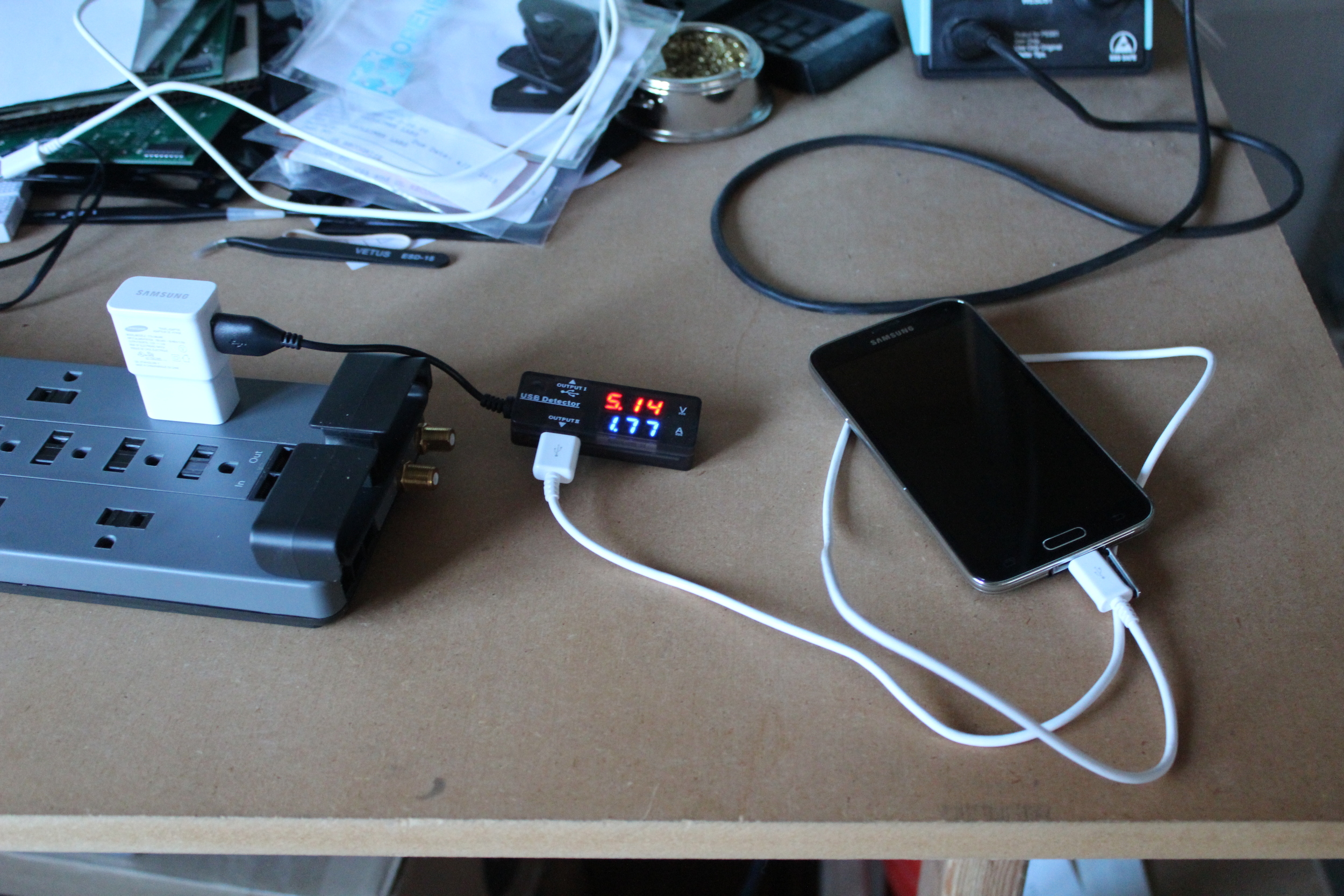
One way to stop these attacks is to use a device that physically disconnects the USB data lines, while leaving the power and ground lines connected. This approach has a major disadvantage because devices and chargers use the data lines to negotiate power requirements, usually via the USB Battery Charging specification. Without that negotiation, the device can’t determine what capabilities the charger has. Instead of being able to draw 7.5 W or more, the device can only safely draw 0.5 W, which means it could take 15 times longer to charge your phone with this technique.

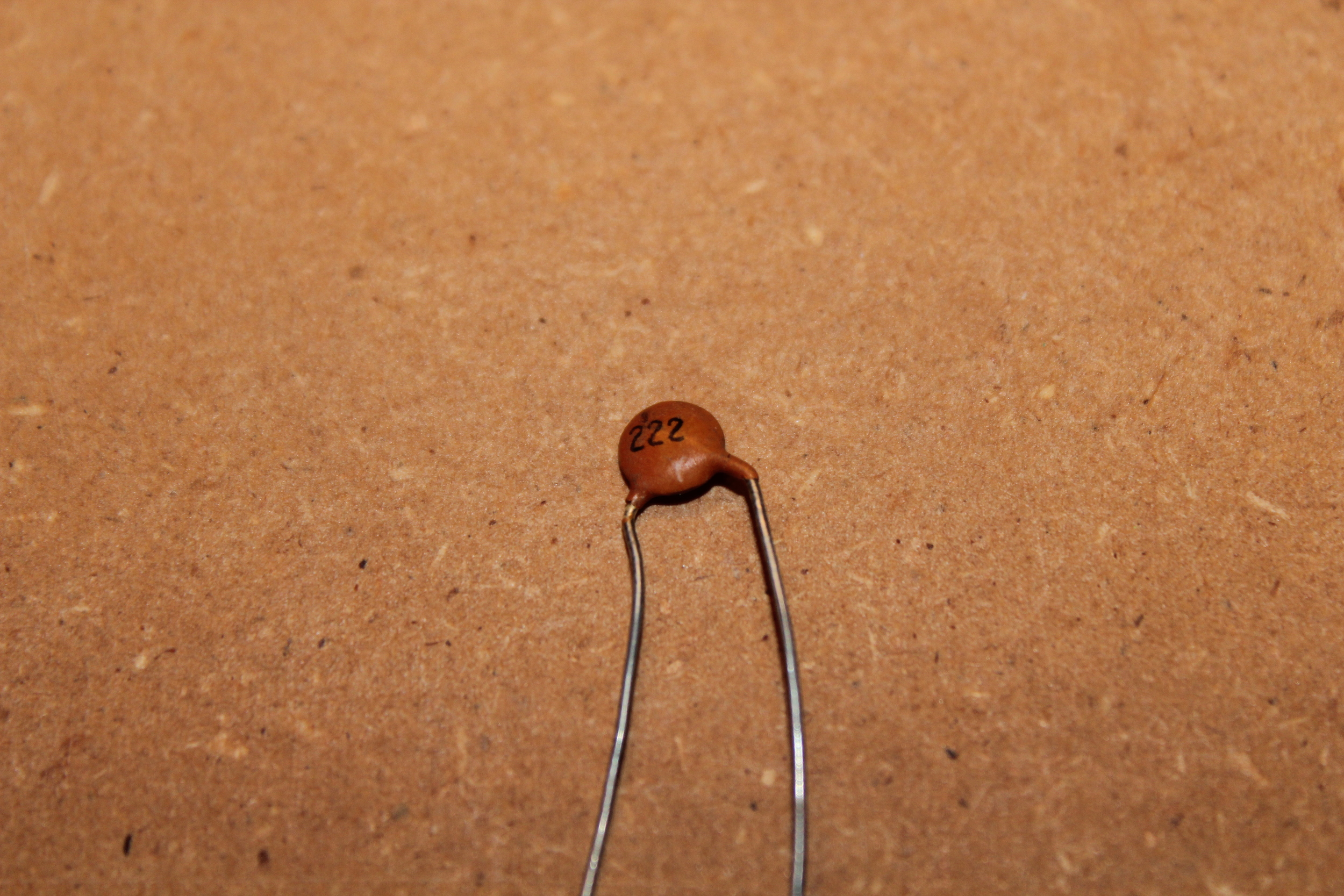
Fortunately, there is a way to block the USB data signals and still allow the device and charger to negotiate the correct amount of power. The key is that the power negotiation occurs much more slowly than the data flow: 100 Hz instead of 1 MHz. A capacitor across either of the data lines limits the bandwidth so that the charging negotiation can occur, but traditional USB data transfers are blocked. In fact, the USB specification has a maximum allowed capacitance between a data line and ground for this reason.

Because the difference in speed from USB Battery Charging to even USB Low Speed is so large, there is plenty of room for error. Anything over 75 pF is outside the official USB spec for data. The data lines have a typical series resistance of 33 Ohms which means a 33 nF capacitor will create an RC filter with a time constant of approximately 1 μs. A time constant of up to 100 μs is acceptable for passing USB Battery Charging signals, and under 0.1 μs is needed for USB Low Spped, so a variety of capacitance values will work.

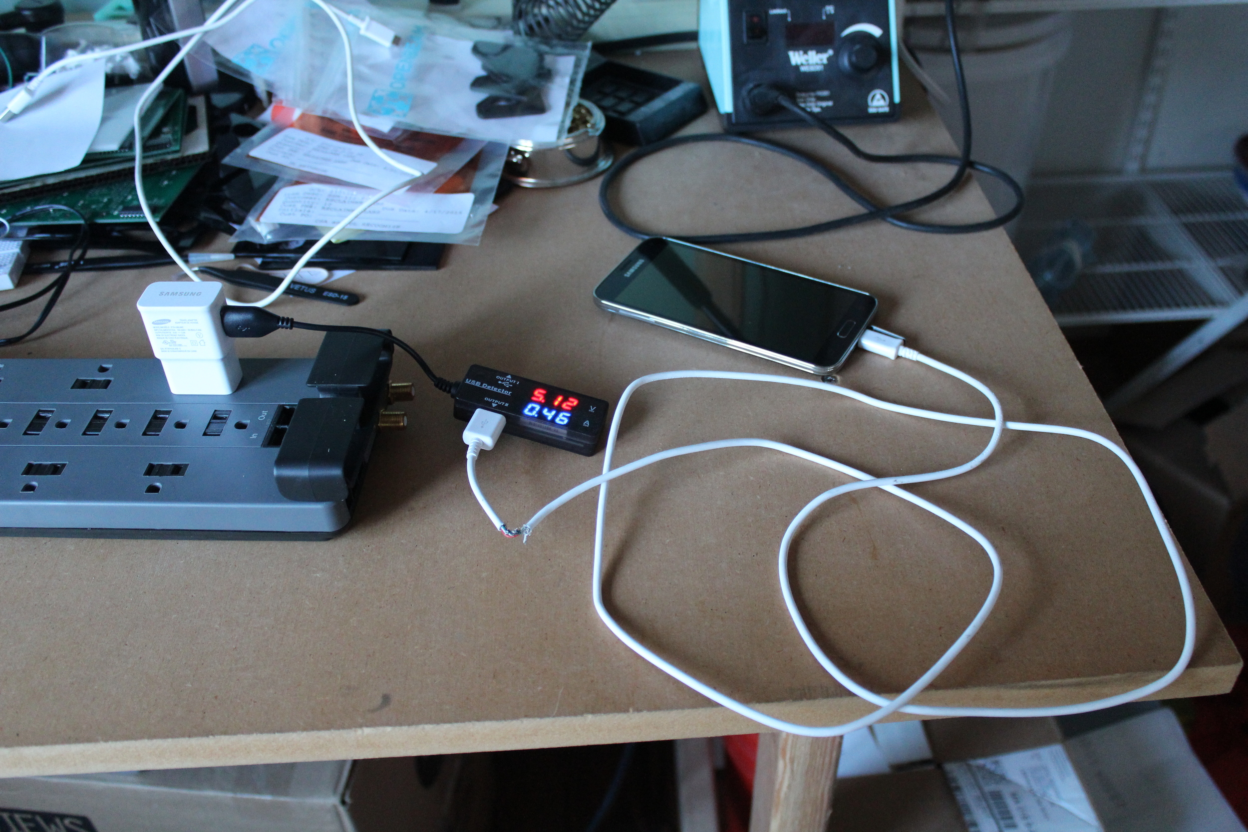
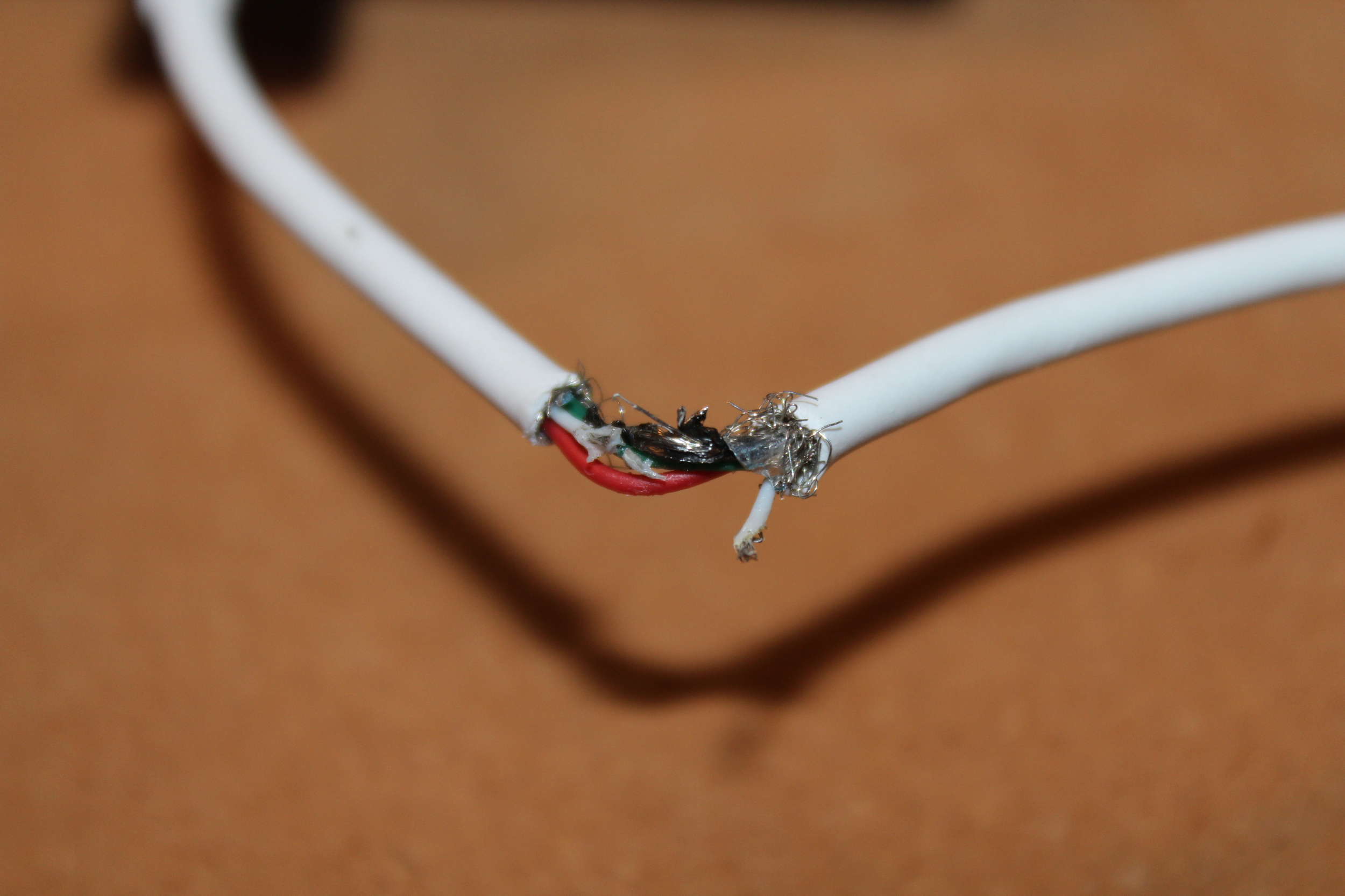
To test my ideas, I ran an experiment. I tried three USB cable configurations and, with each configuration, measured how much power my phone drew and whether or not my desktop recognized the device. I tried the original cable as a control. Then I soldered a 22 nF capacitor between D- and GND. Finally, I cut the D- line entirely. The results are below.

  • Intact cable: 9.1 W - Good connection to desktop
  • Capacitor installed: 7.4 W - "USB Device Unrecognized"
  • D- line cut - 2.4 W: "USB Device Unrecognized"

These results are in line with my expectations. The difference between having the intact cable and having the capacitor installed could result from a difference in battery load. I suspect my phone drew more current than it should have in the third test. It seemed to draw 500 mA instead of 100 mA, which is all that is allowed by the spec. Still, with the D- line connected, it drew significantly less power.

I've designed a small device that incorporates these capacitors, along with some test and debug features, into a small board with a plug on one end and a receptacle on the other. It’s called USB Power Armor. I plan to build prototypes and do further testing this coming week. Here's a preview.

Update: The first units of USB Power Armor Type-A are available for sale now. Click here to get yours.

Using an Arduino

One of the fastest ways to get started with our seven-segment display is to use an Arduino. One Arduino can drive many digits. Up to 10 has been tested. 30 or more is practical with the standard interconnects, and hundreds are possible with multiple power drops.

Hardware

You will need to connect the Arduino to one of your digits. This digit must be on the end of the chain. It will drive the rest of the digits as explained in the firmware section. To connect your Arduino, you have two options:

Use jumper wires

Connect each of the relevant lines between the on-board header and the Arduino. You'll need seven wires. To use the example code, wire up your Arduino according to the following table.

Solder to the on-board pads.

The pads are a bit tight in Rev 3, but they work with the Arduino Uno form factor. You'll need some 0.1 inch male header in right-angle thru-hole, such as Samtec's TSW-120-22-F-S-RA . I recommend putting the header in the Arduino, then soldering the header to the board. Once it's soldered, you can remove the Arduino and replace it at will. See the pictures below.


Firmware

The examples firmware projects are still being developed. Eventually, they will be turned into a firmware library for very fast integration. If you know of an existing library for seven-segment displays, especially for Arduino, please leave a comment.

Each digit takes in data via shift registers. This allows daisy-chaining multiple digits together without the use of additional pins on your Arduino. Adafruit has a great introduction and tutorial for connecting shift registers to an Arduino. The Reclaimer Labs seven-segment display uses the same interface.

To achieve faster speeds and drive more digits, you can use the hardware SPI controller. Although the shift register interface is different than SPI, they are similar enough to be compatible. The most important difference is to ignore the SPI chip select (CS) pin and connect latch enable (LE) to a separate pin. Once all the relevant data has been transmitted, the LE pin must be manually pulled high then low. Using the SPI hardware on your microcontroller can free up the CPU, especially if you have Direct Memory Access (DMA) controllers on-board.

Most of the firmware examples include a font library. You can use this by indexing into the array and shifting out that byte. The index is the value you wish to display. font_inverted[] has values for upside-down digits; font[] is for upside-up. For example, to display a "3" on an inverted digit, you would send the byte font_inverted[3]. To turn on the decimal point, simply set the upper-most bit of the byte. In this example, you would send the byte (font_inverted[3] | (1<<7)).

Summary

This post should be enough to get you started using the seven-segments displays with an Arduino. Feel free to leave a comment or send us an email if you have any questions.

Preproduction Units Available

Preproduction (Rev 3) units of the 6-inch tall seven-segment display are available for sale at the Reclaimer Labs store. All boards are fully assembled and tested. Each segment comes with a laser-cut cardboard waveguide and interconnect. These are early units, so not all the bugs have been worked out. As I update the design to the production design (Rev 4), I will post specifics. In the meantime, you can get started on your projects with these preview units. Enjoy.

Everything included with each segment.

Everything included with each segment.

Preproduction Preview

It's been a while since I updated this blog. That's because I've been working on Rev 3 of the seven segment display. This is the preproduction version. It is an important step on the way to ramping up to mass production. Over the next few weeks I will be testing and evaluating these units and building demos for the Kickstarter video. Stay tuned.

Rev3_back_preview.jpg
Rev3_red_preview.jpg

Prototype Clock

Today I will describe how I built my prototype countdown clock, which counts down to the next SpaceX launch. It automatically updates itself using the Network Time Protocol (NTP) and a script running on my home server. This project will demonstrate how to use the panels and will provide a glimpse into the firmware libraries that are under development.

Counting down to SpaceX DSCOVR launch attempt 1

Counting down to SpaceX DSCOVR launch attempt 1

Interconnect on the prototype clock. Note that only one connection is made.

Interconnect on the prototype clock. Note that only one connection is made.

The hardware consists of the ten Rev 2 prototype displays, one Spark Core, and a breadboard power supply. I’ve connected the digits in pairs to make a colon for every other segment. I used the interconnects along the bottom only. It is important not to connect both top and bottom, which would connect the output of the downstream panels to the input of the panels upstream and cause the display to latch up.

The firmware is experimental, to put it kindly. I threw it together in a weekend, so it’s messy, but I will have time to rework the firmware into a nice library for Spark and Arduino while I wait for the Rev 3 panels. In the meantime, feel free to look at the firmware on Github.

The basic flow of the firmware is to constantly check for the time to advance by a second. It then recalculates the number of seconds until the target time will arrive, does calculations to get the minutes, hours, and days, and then updates the display. Please note that I used the Sparkfun Real Time Clock (RTC) library for Spark, which means that times are not in Unix time but are offset by 2208988800 seconds. This difference confused me for a while. The firmware also includes a function to update the target time. This function can be called at any point by a script on the Internet. I used a string instead of a number because the biggest number I could use was a signed integer, and I wanted to be sure I could represent more distant times if necessary.

The software is even less stable than the firmware. I used Python because I’m familiar with the language and because there are libraries to do everything I needed.  The script downloads the front page of spacexstats.com and then parses it to find the first time, which I assume is the next scheduled launch time. I used Beautiful Soup to do the parsing after referring to a few examples in the documentation. I also found a library to talk to the Spark Cores. To run the script, users will have to install these libraries. Once I had the script, I set up a cron job that runs the script once per minute.

There is much room for improvement in this design, but it was very fun building a working prototype so quickly. Please leave suggestions in the comments or make pull requests on Github.

Using Nail Polish for Soldering

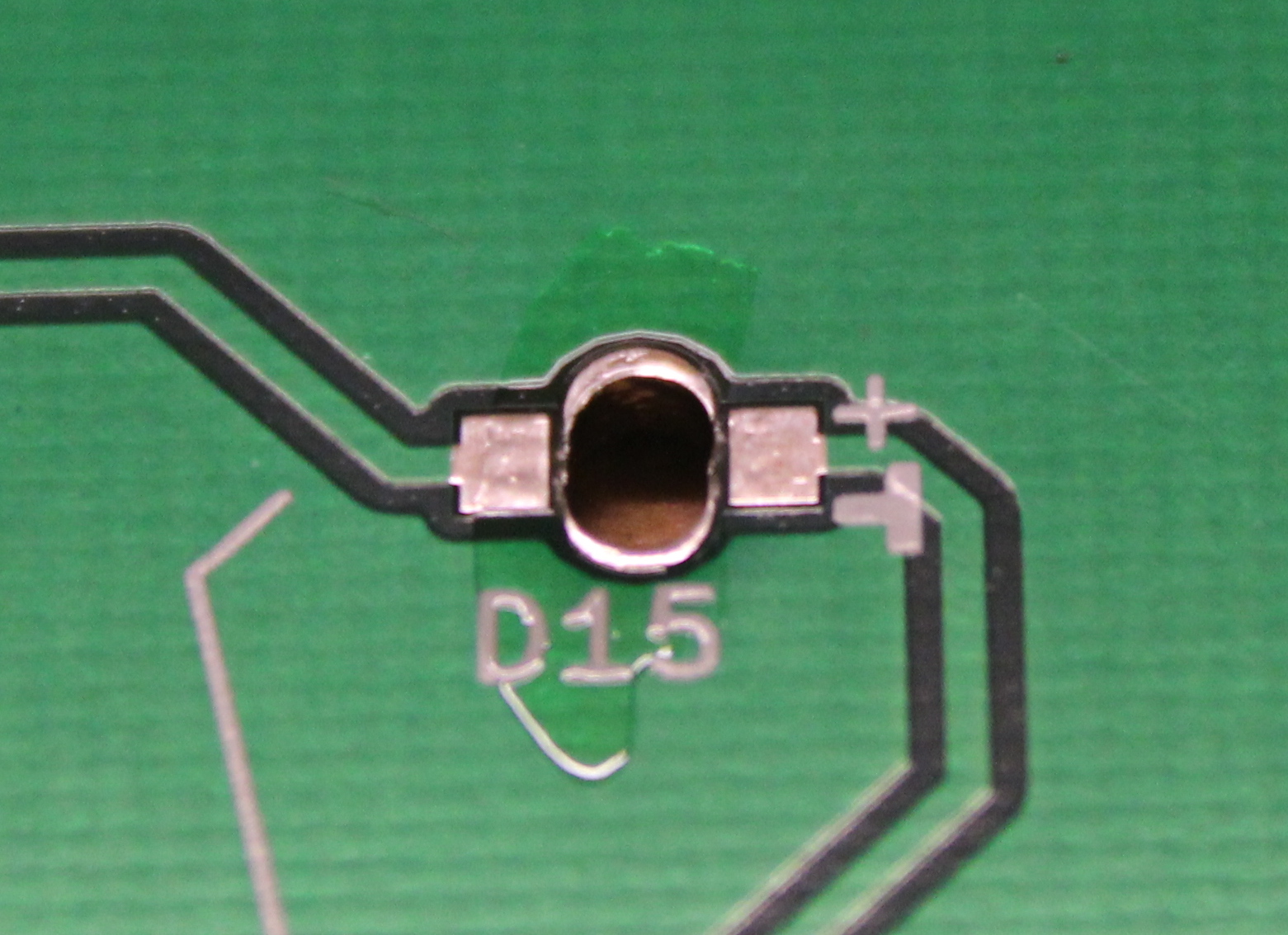
I was having trouble soldering the Rev 2 boards reliably. The major problem involved the slots for the LEDs. For these prototype boards, I needed to stick to a standard PCB fabrication process, which meant that I couldn't get non-plated slots. Unfortunately, plated slots make it very easy to short out the LEDs. To test for a short, I used my multimeter on the diode setting. If the LED lit up, there was no short; if the buzzer beeped, I needed to rework the soldering. Fixing three or four LEDs per board was very time consuming, and it took me 90 minutes to solder the first two boards together. I needed a better solution to cover the plated slots.

At this point, the nail polish came in. I used it as a sort of temporary solder mask. It stinks a bit when the soldering iron hits it, but it's not much worse than the solder itself. Out of the next eight boards, I experienced two shorted LEDs, and that improvement made the process much faster. I'm not convinced nail polish is the best solution, so if you have other suggestions, please leave a comment.